Technology

Top page > Technology

Development Field

Development of 4, 8, 12 and 16 stacked/packaged products using ultra-high speed and ultra-high band width memory design technologies based on extensive experience in developing cutting-edge technologies.
① JEDEC standard DRAM :LP3、LP4、LP5、DDR4、DDR5、HBM
② Custom memory :Wide I/O (x64 or more), multi-channel (4, 8) / package
③ Stacked memory :Wafer on Wafer
④ 2.5, 3D integration
⑤ Ultra-high speed, low power consumption package

Achievements

Original development case
Project Technology Feature Situation
  • Ultra High band width Stacked DRAM
  • Power : Bumpless TSV
  • Signal :TCI
  • WOW stacking
  • Ultra-high bandwidth (1024 bit I/O)
  • Silicon interposerless 3D integration
  • Prototype
  • Evaluation
  • Stacked DDR4
  • Bumpless TSV
  • WOW stacking
  • ×64 DDR4 3200Mbps
  • Mass production
  • (EOL)
  • Custom
  • HBM2E
  • P2P
  • Ultra-high bandwidth
  • Silicon interposerless 3D integration
  • Development
  • Large Capacity
  • Stacked DDR4
  • Power : Bumpless TSV
  • Signal : TCI/Bumpless TSV
  • WOW stacking
  • Large Capacity DDR4 32Gbit/Package
  • High relief efficiency for WOW stacking
  • Development
Memory design service

We have more than 20 design achievements in the development of various memories ( DRAM / SRAM / MRAM ) including custom interfaces.

Patents (Number of registered patents)

As of December 2022, we have registered a total of 43 patents, 22 in Japan, 13 in the United States, and 8 in China.

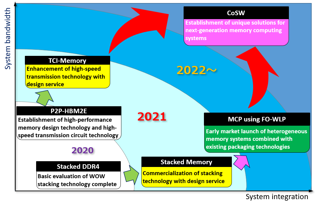
Development Roadmap

ロードマップ
P2P :Pad to Pad interconnect TCI :ThruChip Interface
FO-WLP :Fan Out Wafer Level Package MCP :Multi Chip Package
CoSW :Chip on Stacked Wafer WOW :Wafer on Wafer

Contact us for more information about our technologies.